
Hinge Mechanism
The following is an example done by one of students. The process can be done with 2 polysilicon layers. The topography is a result of the conformal deposition (i.e., good step coverage). You don’t have to perform extra deposition step to create the topography.
(1) Begin with silicon substrate; apply sacrificial layer of SiO2 by low pressure chemical vapor deposition (LPCVD).

(2) First photolithography step: apply a structural layer of polysilicon by LPCVD; pattern, and etch with Cl2‐based plasma etch.
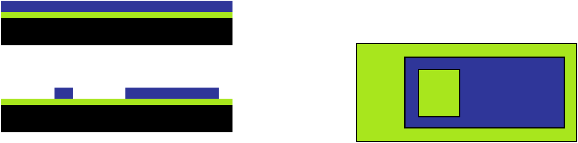
(3) Second photolithography step: apply a second sacrificial oxide layer by LPCVD; pattern, and etch holes through both layersof oxide with CF4 plasma etch.
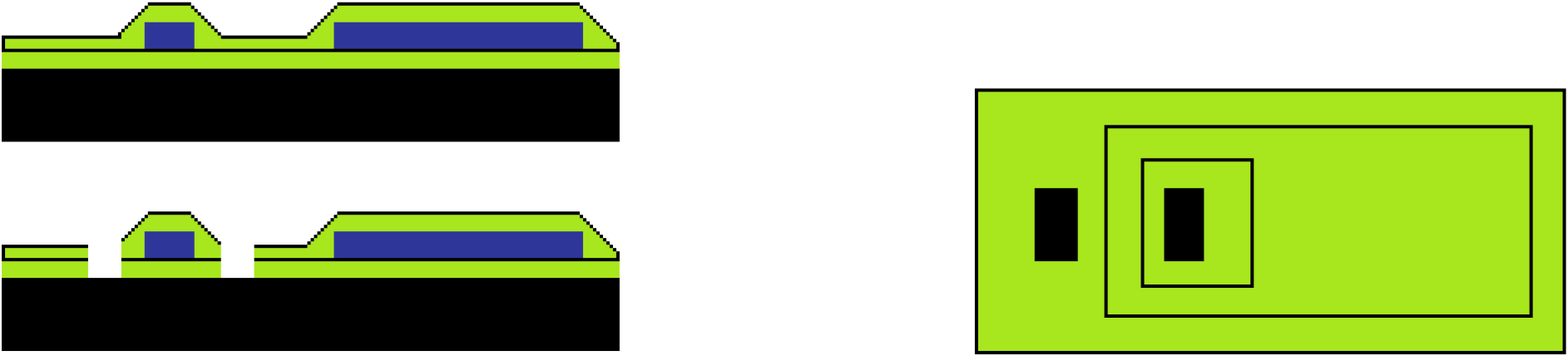
(4) Third photolithography step: apply second structural layer of polysilicon by LPCVD (poly-silicon fills holes to form staple with two anchors); pattern, and etch with Cl2‐based plasma etch.
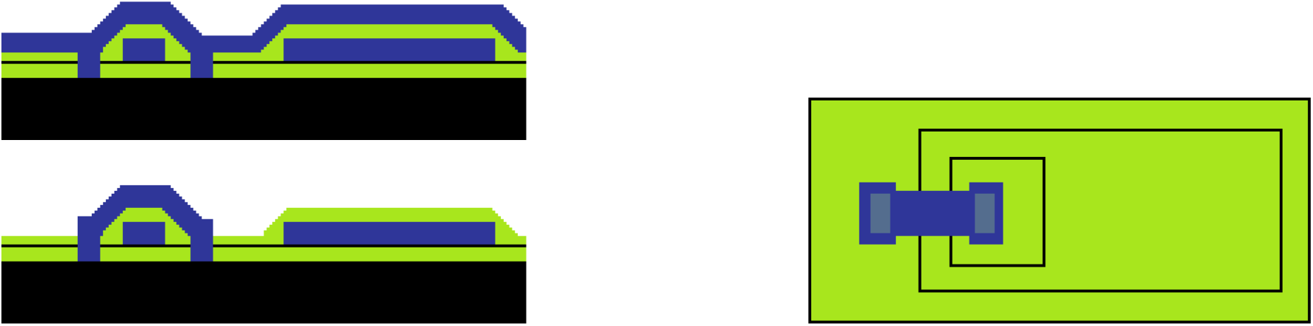
(5) Remove sacrificial oxide layers by HF wet etch, releasing movable polysilicon structures. Dry (may need to take precautions to prevent stiction between structures and substrate).