
Polymerase Chain Reaction (PCR) Chamber
The wafer fabrication uses micromachined silicon, ultrasonically drilled Pyrex glass, and anodic bonding of the two wafers. Metal (Al) heaters and sensors are located on silicon wafer in recessed areas to avoid metal step in bonding. The process flow of the silicon wafer is shown in the figure.
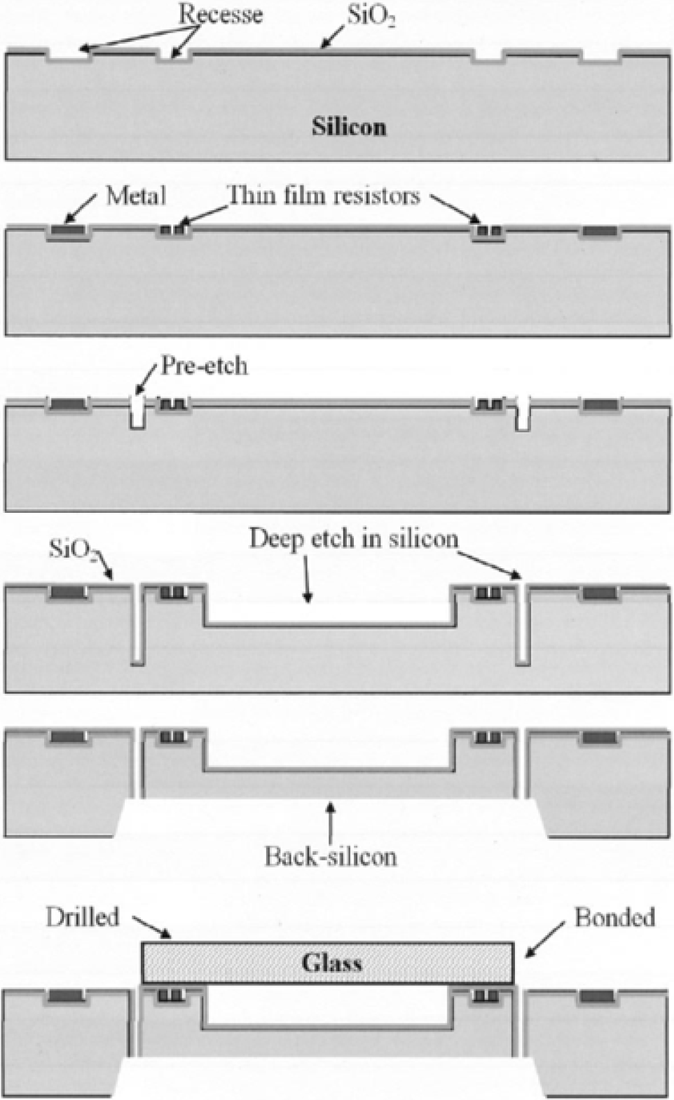
(1) A shallow recess is formed on silicon surface by reactive ion etching (RIE), followed by a thermally grown oxide of 0.1 μm thick.
(2) The aluminum is deposited, patterned and etched, followed by a pre-etching of 50~100 μm deep in silicon as an etch-stop control for the later KOH etch from the backside.
(3) The deep silicon trench etching to a depth of 250~300 μm in channel and chamber areas is performed, to form all the channels, chambers, reservoirs, and valves at the same time, protected by thick photoresist. During this step, the pre-etched trenches are further etched deep into the silicon wafer at the same etch rate.
(4) The resist is stripped, and a second layer of silicon oxide is deposited on top surface by plasma enhanced chemical vapor deposition (PECVD), to form the chemical protection and biocompatible layer for polymerase chain reaction (PCR).
(5) The backside of the silicon wafer is patterned using a double-side aligner and etched to form the anisotropic etching windows, and the backside is etched in a single-side KOH etcher. Once the KOH etch reaches the bottom oxide of the top silicon deep trenches, the etch stops.
(6) The silicon wafer is anodically bonded to a perforated glass wafer. Finally, the bonded wafer is put in a RIE chamber to remove the top oxide on the bond pad areas. The diced chip can be easily attached onto a planar printed circuit board (PCB) or metal plate as the bottom of the chamber is isolated by the formed silicon cavity.

