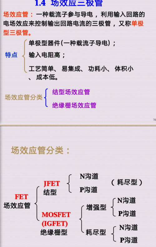
场效应管原理
场效应管是较新型的半导体材料,利用电场效应来控制晶体管的电流,因而得名。它的外型也是一个三极管,因此又称场效应三极管。它只有一种载流子参与导电的半导体器件,是一种用输入电压控制输出电流的半导体器件。从参与导电的载流子来划分,它有电子作为载流子的N沟道器件和空穴作为载流子的P沟道器件。从场效应三极管的结构来划分,它有结型场效应三极管和绝缘栅型场效应三极管之分。
1.结型场效应三极管
(1) 结构
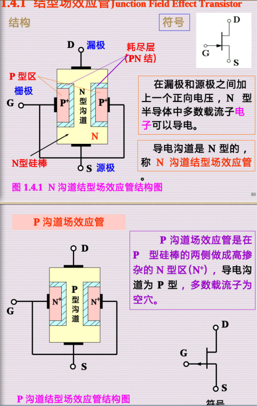
N沟道结型场效应三极管的结构如图1所示,它是在N型半导体硅片的两侧各制造一个PN结,形成两个PN结夹着一个N型沟道的结构。两个P区即为栅极,N型硅的一端是漏极,另一端是源极。

图1结型场效应三极管的结构
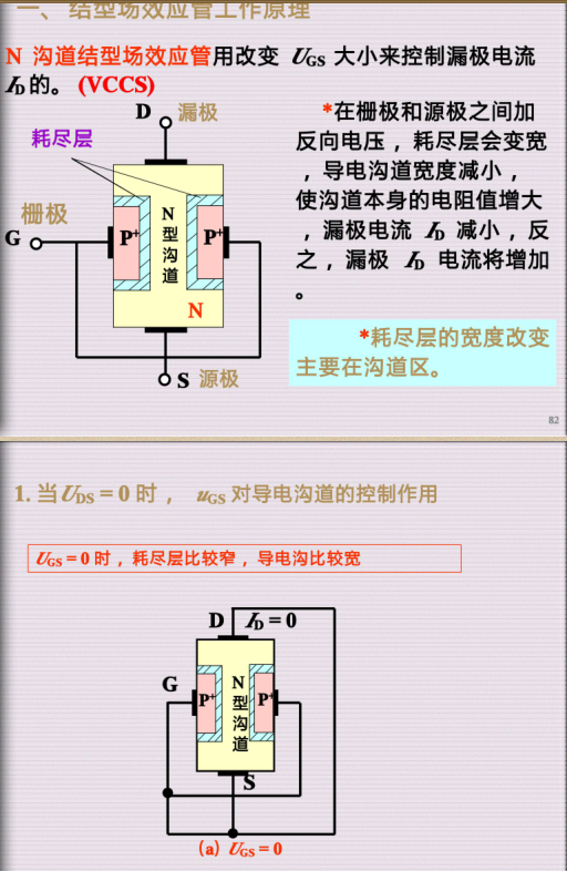
(2) 工作原理
以N沟道为例说明其工作原理。
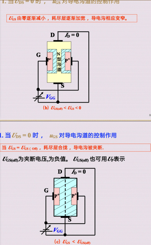
当UGS=0时,在漏、源之间加有一定电压时,在漏源间将形成多子的漂移运动,产生漏极电流。当UGS<0时,PN结反偏,形成耗尽层,漏源间的沟道将变窄,ID将减小,UGS继续减小,沟道继续变窄,ID继续减小直至为0。当漏极电流为零时所对应的栅源电压UGS称为夹断电压UGS(off)。
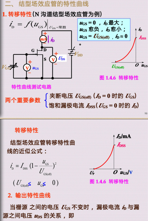
(3)特性曲线
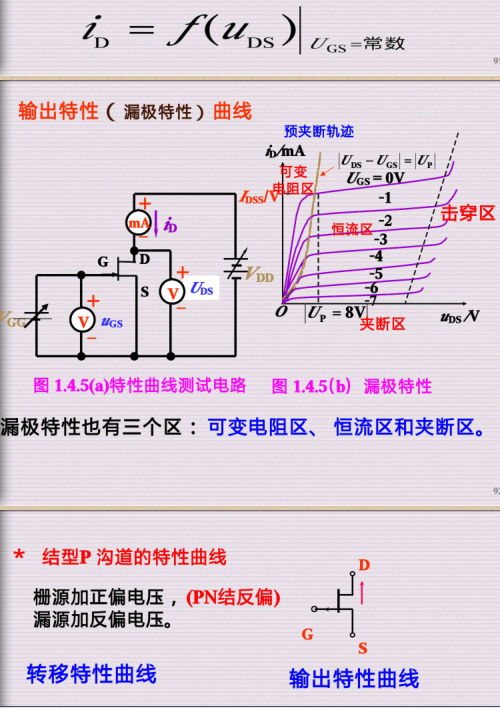
结型场效应三极管的特性曲线有两条,一是输出特性曲线(ID=f(UDS)|UGS=常量),二是转移特性曲线(ID=f(UGS)|UDS=常量)。N沟道结型场效应三极管的特性曲线如图2所示。
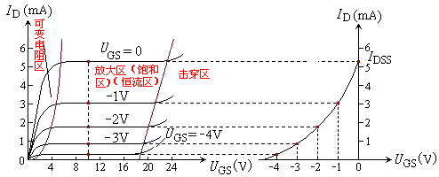
(a) 漏极输出特性曲线 (b) 转移特性曲线
图2N沟道结型场效应三极管的特性曲线
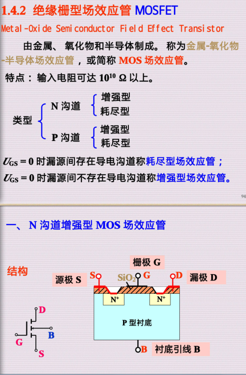
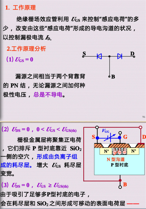
2. 绝缘栅场效应三极管的工作原理
绝缘栅场效应三极管分为:耗尽型 →N沟道、P沟道 增强型 →N沟道、P沟道
(1)N沟道耗尽型绝缘栅场效应管
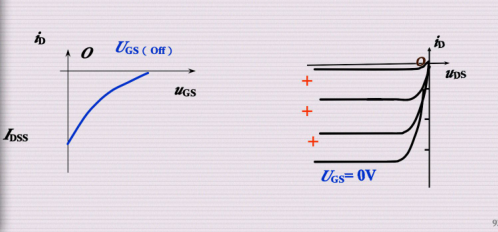
N沟道耗尽型的结构和符号如图3(a)所示,它是在栅极下方的SiO2绝缘层中掺入了大量的金属正离子。所以当UGS=0时,这些正离子已经感应出反型层,形成了沟道。于是,只要有漏源电压,就有漏极电流存在。当UGS>0时,将使ID进一步增加。UGS<0时,随着UGS的减小漏极电流逐渐减小,直至ID=0。对应ID=0的UGS称为夹断电压,用符号UGS(off)表示,有时也用UP表示。N沟道耗尽型的转移特性曲线如图30(b)所示。

(a) 结构示意图 (b) 转移特性曲线
图3N沟道耗尽型绝缘栅场效应管结构和转移特性曲线
(2)N沟道增强型绝缘栅场效应管
结构与耗尽型类似。但当UGS=0 V时,在D、S之间加上电压不会在D、S间形成电流。 当栅极加有电压时,若0UGS(th)时,形成沟道,将漏极和源极沟通。如果此时加有漏源电压,就可以形成漏极电流ID。在UGS=0V时ID=0,只有当UGS>UGS(th)后才会出现漏极电流,这种MOS管称为增强型MOS管。
N沟道增强型MOS管的转移特性曲线,见图4。
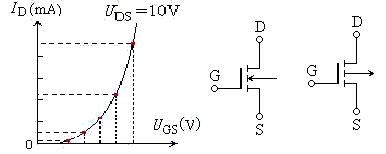
图4转移特性曲线
(3)P沟道MOS管
P沟道MOS管的工作原理与N沟道MOS管完全相同,只不过导电的载流子不同,供电电压极性不同而已。这如同双极型三极管有NPN型和PNP型一样。
3 主要参数
(1) 直流参数
指耗尽型MOS夹断电压UGS=UGS(off) 、增强型MOS管开启电压UGS(th)、耗尽型场效应三极管的饱和漏极电流IDSS(UGS=0时所对应的漏极电流)、输入电阻RGS.
(2) 低频跨导gm
gm可以在转移特性曲线上求取,单位是mS(毫西门子)。
(3) 最大漏极电流IDM
2 场效应半导体三极管
场效应半导体三极管是只有一种载流子参与导电的半导体器件,是一种用输入电压控制输出电流的半导体器件。从参与导电的载流子来划分,它有电子作为载流子的N沟道器件和空穴作为载流子的P沟道器件。从场效应三极管的结构来划分,它有结型场效应三极管JFET(Junction type Field Effect Transister)和绝缘栅型场效应三极管IGFET( Insulated Gate Field Effect Transister) 之分。IGFET也称金属-氧化物-半导体三极管MOSFET (Metal Oxide Semicon-ductor FET)。
2.2.1 绝缘栅场效应三极管的工作原理
绝缘栅场效应三极管(MOSFET)分为:
增强型 →N沟道、P沟道
耗尽型 →N沟道、P沟道
N沟道增强型MOSFET的结构示意图和符号见图02.13。 电极D(Drain)称为漏极,相当双极型三极管的集电极;
G(Gate)称为栅极,相当于的基极;
S(Source)称为源极,相当于发射极。
(1)N沟道增强型MOSFET
① 结构
根据图02.13,N沟道增强型MOSFET基本上是一种左右对称的拓扑结构,它是在P型半导体上生成一层SiO2 薄膜绝缘层,然后用光刻工艺扩散两个高掺杂的N型区,从N型区引出电极,一个是漏极D,一个是源极S。在源极和漏极之间的绝缘层上镀一层金属铝作为栅极G。P型半导体称为衬底,用符号B表示。

图02.13 N沟道增强型MOSFET的结构示意图和符号
② 工作原理
1.栅源电压VGS的控制作用
当VGS=0 V时,漏源之间相当两个背靠背的二极管,在D、S之间加上电压不会在D、S间形成电流。
当栅极加有电压时,若0
进一步增加VGS,当VGS>VGS(th)时( VGS(th) 称为开启电压),由于此时的栅极电压已经比较强,在靠近栅极下方的P型半导体表层中聚集较多的电子,可以形成沟道,将漏极和源极沟通。如果此时加有漏源电压,就可以形成漏极电流ID。在栅极下方形成的导电沟道中的电子,因与P型半导体的载流子空穴极性相反,故称为反型层。随着VGS的继续增加,ID将不断增加。在VGS=0V时ID=0,只有当VGS>VGS(th)后才会出现漏极电流,这种MOS管称为增强型MOS管。
VGS对漏极电流的控制关系可用iD=f(vGS)?VDS=const这一曲线描述,称为转移特性曲线,见图02.14。
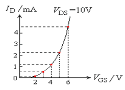
图02.14 转移特性曲线
转移特性曲线的斜率gm的大小反映了栅源电压对漏极电流的控制作用。 gm 的量纲为mA/V,所以gm也称为跨导。
跨导的定义式如下:

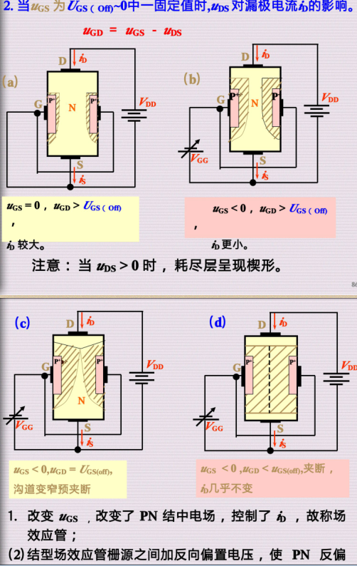
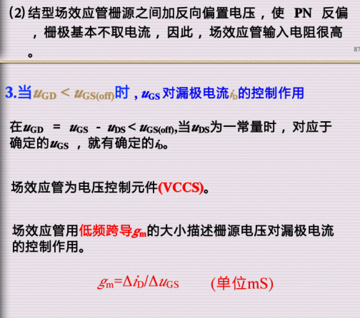
2.漏源电压VDS对漏极电流ID的控制作用
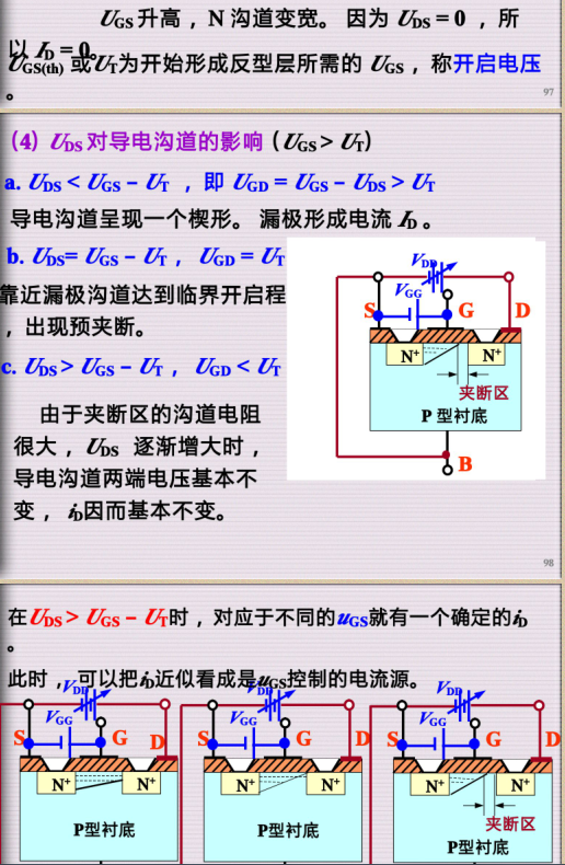
当VGS>VGS(th),且固定为某一值时,来分析漏源电压VDS对漏极电流ID的影响。VDS的不同变化对沟道的影响如图02.15所示。根据此图可以有如下关系
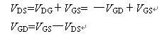
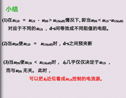
当VDS为0或较小时,相当VGD>VGS(th),沟道分布如图02.15(a),此时VDS 基本均匀降落在沟道中,沟道呈斜线分布。在紧靠漏极处,沟道达到开启的程度以上,漏源之间有电流通过。
当VDS增加到使VGD=VGS(th)时,沟道如图02.15(b)所示。这相当于VDS增加使漏极处沟道缩减到刚刚开启的情况,称为预夹断,此时的漏极电流ID基本饱和。当VDS增加到VGD?VGS(th)时,沟道如图02.15(c)所示。此时预夹断区域加长,伸向S极。 VDS增加的部分基本降落在随之加长的夹断沟道上, ID基本趋于不变。
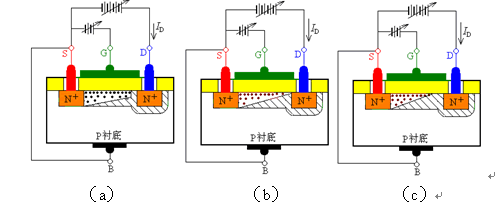
图02.15 漏源电压VDS对沟道的影响(动画2-5)
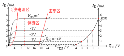
当VGS>VGS(th),且固定为某一值时,VDS对ID的影响,即iD=f(vDS)?VGS=const这一关系曲线如图02.16所示。这一曲线称为漏极输出特性曲线。
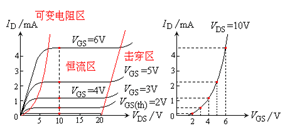
(a) 输出特性曲线 (b)转移特性曲线
图02.16 漏极输出特性曲线和转移特性曲线
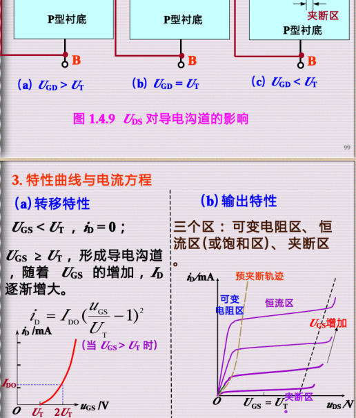
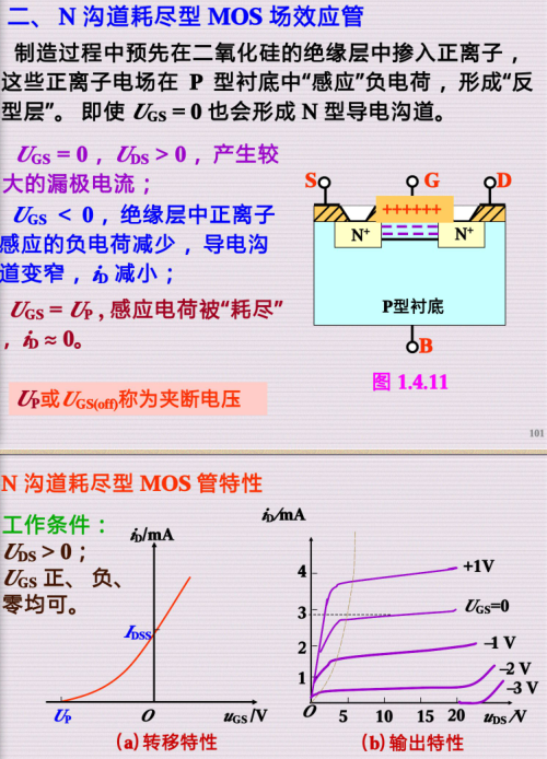
(2)N沟道耗尽型MOSFET
N沟道耗尽型MOSFET的结构和符号如图02.17(a)所示,它是在栅极下方的SiO2绝缘层中掺入了大量的金属正离子。所以当VGS=0时,这些正离子已经感应出反型层,形成了沟道。于是,只要有漏源电压,就有漏极电流存在。当VGS>0时,将使ID进一步增加。VGS<0时,随着VGS的减小漏极电流逐渐减小,直至ID=0。对应ID=0的VGS称为夹断电压,用符号VGS(off)表示,有时也用VP表示。N沟道耗尽型MOSFET的转移特性曲线如图02.17(b)所示。

(a) 结构示意图 (b) 转移特性曲线
图02.17 N沟道耗尽型MOSFET的结构和转移特性曲线
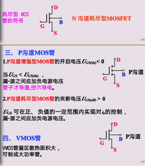
(3)P沟道耗尽型MOSFET
P沟道MOSFET的工作原理与N沟道MOSFET完全相同,只不过导电的载流子不同,供电电压极性不同而已。这如同双极型三极管有NPN型和PNP型一样。
4.2.2 伏安特性曲线
场效应三极管的特性曲线类型比较多,根据导电沟道的不同以及是增强型还是耗尽型可有四种转移特性曲线和输出特性曲线,其电压和电流方向也有所不同。如果按统一规定的正方向,特性曲线就要画在不同的象限。为了便于绘制,将P沟道管子的正方向反过来设定。有关曲线绘于图02.18之中。
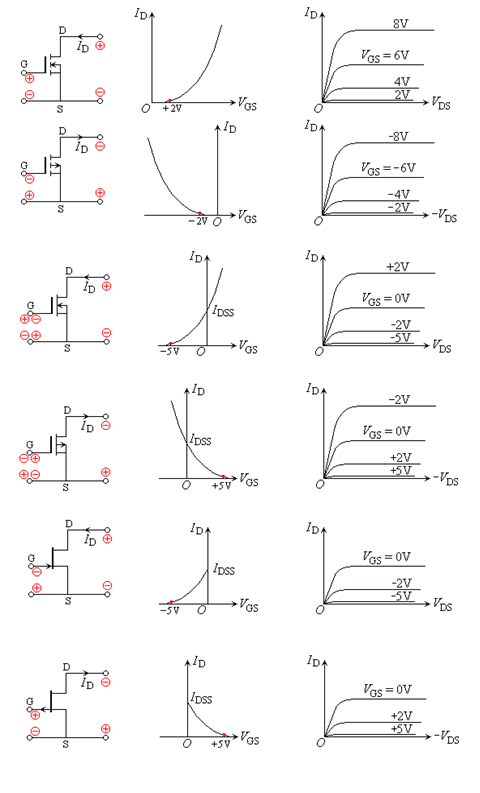
图02.18 各类场效应三极管的特性曲线
4.2.3 结型场效应三极管
(1) 结型场效应三极管的结构
结型场效应三极管的结构与绝缘栅场效应三极管相似,工作机理也相同。结型场效应三极管的结构如图02.19所示,它是在N型半导体硅片的两侧各制造一个PN结,形成两个PN结夹着一个N型沟道的结构。两个P区即为栅极,N型硅的一端是漏极,另一端是源极。
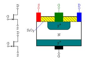
图02.19 结型场效应三极管的结构
(2) 结型场效应三极管的工作原理
根据结型场效应三极管的结构,因它没有绝缘层,只能工作在反偏的条件下,对于N沟道结型场效应三极管只能工作在负栅压区,P沟道的只能工作在正栅压区,否则将会出现栅流。现以N沟道为例说明其工作原理。
① 栅源电压对沟道的控制作用
当VGS=0时,在漏、源之间加有一定电压时,在漏源间将形成多子的漂移运动,产生漏极电流。当VGS<0时,PN结反偏,形成耗尽层,漏源间的沟道将变窄,ID将减小,VGS继续减小,沟道继续变窄,ID继续减小直至为0。当漏极电流为零时所对应的栅源电压VGS称为夹断电压VGS(off)。
② 漏源电压对沟道的控制作用
在栅极加有一定的电压,且VGS>VGS(off),若漏源电压VDS从零开始增加,则VGD=VGS-VDS将随之减小。使靠近漏极处的耗尽层加宽,沟道变窄,从左至右呈楔形分布,如图02.21(a)所示。当VDS增加到使VGD=VGS—VDS=VGS(off)时,在紧靠漏极处出现预夹断,如图02.21(b)所示。当VDS继续增加,漏极处的夹断继续向源极方向生长延长。以上过程与绝缘栅场效应三极管的十分相似。
(3) 结型场效应三极管的特性曲线
结型场效应三极管的特性曲线有两条,一是转移特性曲线,二是输出特性曲线。它与绝缘栅场效应三极管的特性曲线基本相同,只不过绝缘栅场效应管的栅压可正、可负,而结型场效应三极管的栅压只能是P沟道的为正或N沟道的为负。N沟道结型场效应三极管的特性曲线如图02.22所示。
(a) 漏极输出特性曲线(动画2-6) (b) 转移特性曲线(动画2-7)
图02.22 N沟道结型场效应三极管的特性曲线
4.2.4 场效应三极管的参数和型号
(1) 场效应三极管的参数
① 开启电压VGS(th) (或VT)
开启电压是MOS增强型管的参数,栅源电压小于开启电压的绝对值,场效应管不能导通。
② 夹断电压VGS(off) (或VP)
夹断电压是耗尽型FET的参数,当VGS=VGS(off) 时,漏极电流为零。
③ 饱和漏极电流IDSS
耗尽型场效应三极管,当VGS=0时所对应的漏极电流。
④ 输入电阻RGS
场效应三极管的栅源输入电阻的典型值,对于结型场效应三极管,反偏时RGS约大于107Ω,对于绝缘栅场型效应三极管,RGS约是109~1015Ω。
⑤ 低频跨导gm
低频跨导反映了栅压对漏极电流的控制作用,这一点与电子管的控制作用十分相像。gm可以在转移特性曲线上求取,单位是mS(毫西门子)。
⑥ 最大漏极功耗PDM
最大漏极功耗可由PDM= VDS ID决定,与双极型三极管的PCM相当。
(2) 场效应三极管的型号
场效应三极管的型号,现行有两种命名方法。其一是与双极型三极管相同,第三位字母J代表结型场效应管,O代表绝缘栅场效应管。第二位字母代表材料,D是P型硅,反型层是N沟道;C是N型硅P沟道。例如,3DJ6D是结型N沟道场效应三极管,3DO6C是绝缘栅型N沟道场效应三极管。
第二种命名方法是CS××#,CS代表场效应管,××以数字代表型号的序号,#用字母代表同一型号中的不同规格。例如,CS14A、CS45G等。
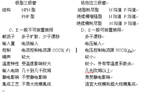
4.2.5 双极型和场效应型三极管的比较
场效应管外文资料 (里面用手捏软管实在是太形象了,超赞,建议看看。果然老外的思想和超爹我上课一样飘逸,富有想象力,)
来源于:https://www.allaboutcircuits.com/textbook/semiconductors/chpt-5/junction-field-effect-transistors-jfet/
Introduction to Junction Field-effect Transistors (JFET)
Chapter 5 - Junction Field-effect Transistors
A transistor is a linear semiconductor device that controls current with the application of a lower-power electrical signal. Transistors may be roughly grouped into two major divisions: bipolar and field-effect. In the last chapter, we studied bipolar transistors, which utilize a small current to control a large current. In this chapter, we’ll introduce the general concept of the field-effect transistor—a device utilizing a small voltage to control current—and then focus on one particular type: the junction field-effect transistor. In the next chapter, we’ll explore another type of field-effect transistor, the insulated gate variety.
All field-effect transistors are unipolar rather than bipolar devices. That is, the main current through them is comprised either of electrons through an N-type semiconductor or holes through a P-type semiconductor. This becomes more evident when a physical diagram of the device is seen:

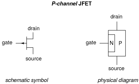
In a junction field-effect transistor or JFET, the controlled current passes from source to drain, or from drain to source as the case may be. The controlling voltage is applied between the gate and source. Note how the current does not have to cross through a PN junction on its way between source and drain: the path (called a channel) is an uninterrupted block of semiconductor material. In the image just shown, this channel is an N-type semiconductor. P-type channel JFETs are also manufactured:
Generally, N-channel JFETs are more commonly used than P-channel. The reasons for this have to do with obscure details of semiconductor theory, which I’d rather not discuss in this chapter. As with bipolar transistors, I believe the best way to introduce field-effect transistor usage is to avoid theory whenever possible and concentrate instead on operational characteristics. The only practical difference between N- and P-channel JFETs you need to concern yourself with now is biasing of the PN junction formed between the gate material and the channel.
With no voltage applied between gate and source, the channel is a wide-open path for electrons to flow. However, if a voltage is applied between gate and source of such polarity that it reverse-biases the PN junction, the flow between source and drain connections becomes limited or regulated, just as it was for bipolar transistors with a set amount of base current. Maximum gate-source voltage “pinches off” all current through source and drain, thus forcing the JFET into cutoff mode. This behavior is due to the depletion region of the PN junction expanding under the influence of a reverse-bias voltage, eventually occupying the entire width of the channel if the voltage is great enough. This action may be likened to reducing the flow of a liquid through a flexible hose by squeezing it: with enough force, the hose will be constricted enough to completely block the flow.

Note how this operational behavior is exactly opposite of the bipolar junction transistor. Bipolar transistors are normally-off devices: no current through the base, no current through the collector or the emitter. JFETs, on the other hand, are normally-on devices: no voltage applied to the gate allows maximum current through the source and drain. Also, take note that the amount of current allowed through a JFET is determined by a voltage signal rather than a current signal as with bipolar transistors. In fact, with the gate-source PN junction reverse-biased, there should be nearly zero current through the gate connection. For this reason, we classify the JFET as a voltage-controlled device and the bipolar transistor as a current-controlled device.
If the gate-source PN junction is forward-biased with a small voltage, the JFET channel will “open” a little more to allow greater currents through. However, the PN junction of a JFET is not built to handle any substantial current itself, and thus it is not recommended to forward-bias the junction under any circumstances.
This is a very condensed overview of JFET operation. In the next section, we’ll explore the use of the JFET as a switching device.
The Junction Field-effect Transistor (JFET) as a Switch
Chapter 5 - Junction Field-effect Transistors
Like its bipolar cousin, the field-effect transistor may be used as an on/off switch controlling electrical power to a load. Let’s begin our investigation of the JFET as a switch with our familiar switch/lamp circuit:

Remembering that the controlled current in a JFET flows between source and drain, we substitute the source and drain connections of a JFET for the two ends of the switch in the above circuit:

If you haven’t noticed by now, the source and drain connections on a JFET look identical on the schematic symbol. Unlike the bipolar junction transistor where the emitter is clearly distinguished from the collector by the arrowhead, a JFET’s source and drain lines both run perpendicular into the bar representing the semiconductor channel. This is no accident, as the source and drain lines of a JFET are often interchangeable in practice! In other words, JFETs are usually able to handle channel current in either direction, from source to drain or from drain to source.
Now, all we need in the circuit is a way to control the JFET’s conduction. With zero applied voltage between gate and source, the JFET’s channel will be “open,” allowing full current to the lamp. In order to turn the lamp off, we will need to connect another source of DC voltage between the gate and source connections of the JFET like this:

Closing this switch will “pinch off” the JFET’s channel, thus forcing it into cutoff and turning the lamp off:

Note that there is no current going through the gate. As a reverse-biased PN junction, it firmly opposes the flow of any electrons through it. As a voltage-controlled device, the JFET requires negligible input current. This is an advantageous trait of the JFET over the bipolar transistor: there is virtually zero power required of the controlling signal.
Opening the control switch again should disconnect the reverse-biasing DC voltage from the gate, thus allowing the transistor to turn back on. Ideally, anyway, this is how it works. In practice this may not work at all:

Why is this? Why doesn’t the JFET’s channel open up again and allow lamp current through like it did before with no voltage applied between gate and source? The answer lies in the operation of the reverse-biased gate-source junction. The depletion region within that junction acts as an insulating barrier separating gate from source. As such, it possesses a certain amount of capacitance capable of storing an electric charge potential. After this junction has been forcibly reverse-biased by the application of an external voltage, it will tend to hold that reverse-biasing voltage as a stored charge even after the source of that voltage has been disconnected. What is needed to turn the JFET on again is to bleed off that stored charge between the gate and source through a resistor:

This resistor’s value is not very important. The capacitance of the JFET’s gate-source junction is very small, and so even a rather high-value bleed resistor creates a fast RC time constant, allowing the transistor to resume conduction with little delay once the switch is opened.
Like the bipolar transistor, it matters little where or what the controlling voltage comes from. We could use a solar cell, thermocouple, or any other sort of voltage-generating device to supply the voltage controlling the JFET’s conduction. All that is required of a voltage source for JFET switch operation is sufficient voltage to achieve pinch-off of the JFET channel. This level is usually in the realm of a few volts DC, and is termed the pinch-off or cutoff voltage. The exact pinch-off voltage for any given JFET is a function of its unique design, and is not a universal figure like 0.7 volts is for a silicon BJT’s base-emitter junction voltage.
REVIEW:
Field-effect transistors control the current between source and drain connections by a voltage applied between the gate and source. In a junction field-effect transistor (JFET), there is a PN junction between the gate and source which is normally reverse-biased for control of source-drain current.
JFETs are normally-on (normally-saturated) devices. The application of a reverse-biasing voltage between gate and source causes the depletion region of that junction to expand, thereby “pinching off” the channel between source and drain through which the controlled current travels.
It may be necessary to attach a “bleed-off” resistor between gate and source to discharge the stored charge built up across the junction’s natural capacitance when the controlling voltage is removed. Otherwise, a charge may remain to keep the JFET in cutoff mode even after the voltage source has been disconnected.